- Table of contents
- PCIe(PCI Express)
- Components and blocks
- Connectors
- The PCB
https://www.youtube.com/watch?v=THLdycw9-Vs
PCIe(PCI Express)
- PCI Express® Base Specification Revision 4.0 Version 1.0
- PCI Express Card Electromechanical Specification Revision 4.0, Version 0.9
Components and blocks
FPGA
Xilinx documentations and datasheets :- XA Artix-7 FPGAs Data Sheet: Overview
- 7 Series FPGAs SelectIO Resources User Guide
- 7 Series FPGA Packaging and Pinout Specification
- 7 Series FPGAs GTP Transceiver User Guide
- 7 Series FPGAs PCB Design and Pin Planning Guide
- 7 Series FPGAs Memory Interface Solutions User Guide
- 7 Series FPGAs and Zynq-7000 AP SoC XADC Dual 12-Bit 1 MSPS Analog-to-Digital Converter
- 7 Series FPGA Configuration User Guide
- Artix‐7 FPGAs Data Sheet: DC and AC Switching Characteristics
- Reducing System BOM Cost with Xilinx's Cost-Optimized Portfolio
- DDR2/DDR3 Low-Cost PCB Design Guidelines for Artix-7 and Spartan-7 FPGAs
- Vivado Design Suite User Guide: Programming and Debugging
- Arty A7-100T schematic and manual
- Alinx AX7101 dev board
- Artix7 Reference designs
- Renesas' Xilinx Artix 7 High current power and timing Slidedeck
- Renesas' Application note for Artix7 and Zynq7000
- Antmicro Releases an Open-Hardware Development Board for AMD Xilinx's Kintex-7 K410T FPGA
Configuration
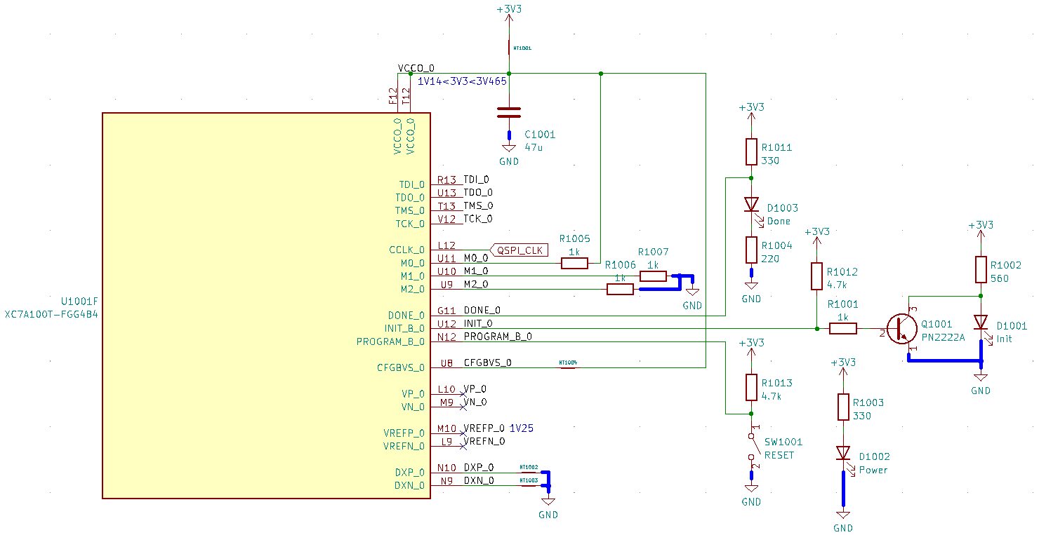
The FPGA can be configured by several means. It can received a pushed configuration from an external device such as a microcontroller, it can pull its configuration from an external device such as a flash memory, or it can be configured using the JTAG connection. Whatever happens, the JTAG always has priority. Thus, I chose to store the configuration in an external Quad-SPI flash. This FPGA device (Artix7 100T) needs 30Mbit to store the whole configuration and would need several seconds to initialize with standard SPI. I chose to use Quad-SPI flash to remain in a reasonnable configuration time, at a reasonnable cost and complexity. Unfortunately, there is a drawback, it would be too complex to access both the FPGA and the flash from the same connector (either JTAG or PCI). The Flash is behind the FPGA and not directly accessible. The programmer needs to configure the FPGA with a temporary bitstream which will act as a flash programmer, this is called indirect programming.
I need to configure the mode pins (M0, M1, M2 in bank 0) to tell the FPGA to fetch its configuration from the SPI flash. I hardwire this value because JTAG programming will still have the priority. The FPGA generate the QSPI clock signal to drive the QSPI flash on pin CCLK_0). Then I need to choose and connect the QSPI flash memory to the relevant pins in bank 14 (data lines and chip select). I do not have to care about the generated clock frequency, the FPGA will start slowly and the very first bits in the downloaded bitstream can increase the generated clock freqency dynamically. Which is very flexible to chose the actual QSPI flash chip.
The QSPI voltage levels have to be consistent across the different pins (CCLK_0 on bank 0, and the other pins on bank 14), the banks need to have the same voltage, at least during the configuration stage. I chose to power the banks 0, 14 and 15 (side effect) at 3.3V, This range is configured with the CFGBVS pin.
The PROGRAM pin acts as a reset an reacts to a pulse (it can not keep the FPGA in reset state). I connected it to a manual reset push button.
When the FPGA is started or reseted, before storing his configuration, it has to reset and clean its current configuration. The INIT_0 pin is switched to LOW during this cleanup and reverts to HIGH after to start the actual configuration. It is possible to keep it LOW and keep the FPGA in reset state.
Once the configuration is loaded, the DONE_0 pin is bring HIGH.
I connected LEDs to INIT_0 and DONE_0 as status indicators to follow and debug the reset and configuration stages.
Power needs
From Artix7 datasheet summary| Name | Min. | Typ. | Max. | Load | Decoupling | Comments |
|---|---|---|---|---|---|---|
| VCCINT | 0.95V | 1.00V | 1.05V | 0.3-6A | 1x330uF, 6x4.7uF, 8x0.47uF | Same rail |
| VCCBRAM | 0.95V | 1.00V | 1.05V | 0.1A | 1x100uF, 2x0.47uF | |
| VCCAUX | 1.71V | 1.80V | 1.89V | 0.15-0.35A | 1x47uF, 3x4.7uF, 5x0.47uF | |
| VCCO | 1.14V | 3.465V | 0.2-2.5A | Bank0: 1x47uF, Other banks: 1x100uF, 2x4.7uF, 4x0.47uF | ||
| VMGTAVCC | 0.97V | 1.00V | 1.03V | 0.15-1A | Has to be filtered accordingly to 7 Series FPGAs GTP Transceiver User Guide (UG482) | |
| VMGTAVTT | 1.17V | 1.20V | 1.23V | 0.05-0.4A | ||
| VCCADC | 1.71V | 1.80V | 1.89V | 0.15-0.35A | ||
| VREFP | 1.20V | 1.25V | 1.30V | |||
| VCCBATT | 1.00V | 1.89V | Battery required only if encryption, otherwise : connect to GND or VCCAUX | |||
| VIN | -0.20V | VCCO+0.20V |
(1*6)+(1*.1)+(1.8*.35)+(3.465*2.5)+(1*1)+(1.2*.4)+(1.8*.35) = 17.5W
The FPGA could theorically consume approximately 17.5W with mixed voltages. The different voltages can not easily be generated directly from the available 12V. We need a first DC/DC conversion from 12V to 5-5.5V and a second from 5-5.5V to the different voltages. Thus, with an efficiency of 80% for each converter, we need approximately :
- 5-5.5V at 4.38A for the second stage (17.5W/80%/5V = 4.38A)
- 12V at 2.28A for the first stage. (17.5W/.8/80%/12V = 2.28A)
The card will also have network, RAM, SPI Flash, ... Despite the PCIe bus provided 12V/2.1A would be sufficient in most cases, I will add an extra power connector to use the ATX 12V/6.5A if available.
Decoupling capacitor recommendations (Types, ESL, ESR, and suggestions available in UG483)| Value | Package | Volts |
|---|---|---|
| 330uF | 2917 | 2.5V |
| 100uF | 1210 | 2.5V |
| 47uF | 1210 | 6.3V |
| 4.7uF | 0805 | 6.3V |
| 0.47uF | 0603 | 6.3V |
the JTAG connector
The card will be tested and used as a development board first. Thus, it needs to be configurable with a JTAG connector. The easiest way is to remain compatible with Xilinx's connector. Their ribbon cable has 14 pins, with an IDC connector. I added a very simple ESD protection.
I might switch later to a smaller JTAG connector with pogo pins, such as the TAG-Connects'
Power supplies
On standard (micro)ATX motherboards, there is a limited power available through the 3.3V and 12V rails. The ATX standard also includes extra 12V power connectors for graphic cards.
There are five possible power sources for the PCIe format :- The PCIe connector 3.3V at 3A (9.9W)
- The PCIe connector 12V at 0.5A, 2.1A or 5.5A depending on the size and software configuration
- An ATX 6-pins 12V/6.25A (75W)
- An ATX 6-pins 12V/6.25A (75W)
- An ATX 8-pins 12V/12.5A (150W)
There are some limitations :
- PCIe x1 : limited to 0.5A (6 W)
- PCIe x4 : limited to 2.1A (25 W)
- PCIe x16: up to 5.5A (66 W), if software configured as an high-power device. Despite the card is in the PCIe format, it has to fit in a backplane, which may not implement this logic
- up to 2 x 6-pins connectors to provide additional 12V (75W each)
- up to 1 x 8 pins connector to provide additional 12V (150W)
Thus, I choose to use a PCIe x16 connector to be safe. If the motherboard can be configured to deliver 5.5A, fine, if not, it can deliver 2.1A at least. In addition, I add an ATX 6pin connector to use it as a main power source, when connected, to avoid any stress on the motherboard.
Automatic power source switch
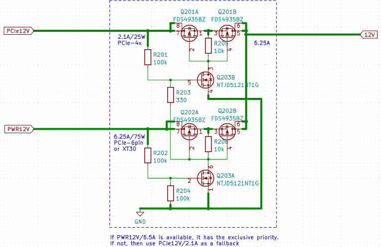
For simplicity, I do not plan to use combined power supplies. The card can use more than the 25W provided by default by the 12V PCIe connector. It needs to automatically switch to a more powerfull power source, when available. The card should use the extra connector 12V if available, then the PCIe provided 12V as a fallback, with automatic switching.
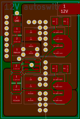
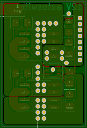
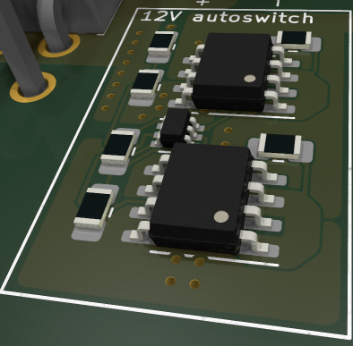
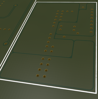
I designed an automated switching circuit, based on two P-channel MOSFETs, used as an ideal diodes to avoid voltage drop and as switches, per power source. They are drived by smaller N-Channel MOSFETs to implement the priority chain. Extra care was taken during the PCB layout design to dissipate as much heat as I can.
Online simulator
PCB and assembly files sent to the manufacturer: PowerSwitchModule-production.zip
- It goes to GND through R8 and R11, acting as a voltage divider. The middle voltage is greater than Q3B's V GS (TH) and unblock it.
- Tt goes through Q2A using the internal diode, is blocked by Q2B's diode. It goes through R13, acting as a pullup resistor, and goes to GND through Q3B.
- Q2A and Q2B gates are low, unblocking them. The current continues to flow through Q2A, bypassing the internal diode and its voltage drop, and both through the R13 pullup resistor and through Q2B to the 12V output.
- Whatever voltage is PCIe12V, the voltage divider R7-R9 is connected to GND through Q3B and Q3A's gate is too low to unblock the MOSFET.
- If PCIe12V is high, the current goes through Q1A's diode, is blocked by Q1B and Q3A, Q1A and Q1B's gates are high, the MOSFETs are blocked
- If PCIe12V is low, the current can flow from the 12V output through Q1B's internal diode, but is blocked by Q1A's diode and can not flow to the PCIe12V source.
- The system is stable with a 12V output from PWR12V
The design could be simplified at the PWR12V level, given that this is the highest priority source, it should not be disabled by something else. I chose to keep it, in order to have a scalable design, in case of additional power sources, in case of a soft start, in case of a power switch, ....
Component and values choices : we have to keep in mind the limited availability of some components, currently, and the prices.
Q1A/Q1B need :- V DSS > 12V,
- V GS > 12V,
- V ~GS (TH) < 12V
- I DS > 2.1A
- V DSS > 12V,
- V GS > 12V,
- V ~GS (TH) < 12V
- I DS > 6.25A
- V DSS > 12V,
- V GS > 12V,
- V ~GS (TH) < 12V
- I DS > current flowing through R12/R13
- high values for low current leakage
- voltage < Q3A's V GS (TH) when Q3B is unblocked
- voltage > Q3A's V GS (TH) when Q3B is unblocked (floating)
- high values for low current leakage
- voltage > Q3B's V GS (TH)
- pullup resistors
- high enought for small current leakage
- R = U/I = 12V / 1mA = 12k. I chose 10k, this is a standard value for pullup/pulldown
I chose the same dual-PMOS chip for both Q1 and Q2, to limit the BOM length at the price of few extra cents and an oversized Q1.
Inspired by :- https://www.youtube.com/watch?v=3e8UgoE1VUc
- https://www.youtube.com/watch?v=nSSvULy_Nd0
- https://www.youtube.com/watch?v=_JM1JVIn7Zo
12V -> 5V5/5A DC/DC step-down
TODO
Inductance choice : https://www.youtube.com/watch?v=ki32ZtKWe_Q
https://www.youtube.com/watch?v=FqT_Ofd54fo
- Input: 12V
- Output: 5.5V/5A
- MPS,
- TI,
- DA,
- ...
- Monolithic Power Systems MP4462DN-LF-Z
- Monolithic Power Systems MP9486AGN-Z
- Texas Instruments TPS54331DR
The first one is fine enough and 0.20€ cheaper, still in production, available in QFN and SOIC packages, simple to implement with few components, has a programable switching frequancy between 200kHz and 4MHz. It can sustain 3.5A with a current limiter between 4 and 4.7A. Last but not least, it has an excellent documentation. Its only disadvantage is that it is an "extended part" at JLCPCB, meaning manual feeding and extra cost (x5 on average).
The third one has the huge advantage of being highly available at JLCPCB, as a "basic part" (no manual intervention, already in the feeders).
MPQ9633B:- few external components
- relatively easy to implement
- not too expensive
- available
- C IN1 = C IN2 = 470uF (SMD 2917)
- C IN3 = 47uF (SMD 1206)
Low voltage power supplies
We need the following rails to power the FPGA :- VCCINT for internal logic
- VCCBRAM for the BRAM cells, which can be consolidated with VCCINT
- VCCAUX
- VCCOx for each of the banks 0,13,14,15,34,35)
- VCCBATT for the batterie used to keep the AES private key used to decrypt bitstream, in the FPGA
- VMGTAVCC for the transceivers
- VMGTAVTT for the transceivers
- VCCADC for the ADC ?
- VREFP for the ADC ?
It is possible to use a complex circuit with a lot of cheap and easy to buy discrete components and simple ICs, but it means a lot of components to order, a complex routing on the PCB, a lot of very small components to solder. On the other hand, I can use few and expensive complex components, which are harder to find, but the PCB routing will be easier, there will be less soldering.
The Reducing System BOM Cost with Xilinx's Cost-Optimized Portfolio whitepaper provides SMPS suggestions (Dialog DA9062, Monolithic Power Systems MP5416, Exar/MaxLinear XRP7714, Texas Instruments TPS65023), furthermore, the Arty A7 and the AX7101 schematics also provide some good inspirations.
The main power source is the PCI express slot. I can not use the permanent 3.3V, I need to use the 12V. Either I can find a suitable component which can accept 12V input or I need to use some kind of step-down from 12V to 5.5V (I added some extra headroom for LDO dropout, in case).
- Exar/MaxLinear XRP7714 is discarded because it has only 4 outputs, and would need extra components to get all the required voltages.
- Texas Instruments TPS65023 is discarded because it can provide less current, probably not enough to make a reasonable use of the FPGA.
- Dialog DA9062 has enough outputs, enough power (up to 8.5A combined), a good set of features (watchdog, RTC, timers, power on/off sequences, ...) and a very comprehensive documentation.
- Monolithic Power Systems MP5416 has one more LDO, very interesting power (approx 15A), with a lot of features (but no RTC).
- how many external components needed ?
- how easy to find and buy ?
- how cheap/expensive ?
MP5416 is nearly impossible to find. Dialog DA9062 is not easy to find, but possible. That's also the PMIC used in Digilent's Arty A7 dev board.
RAM
Storage
The RAM storage has to be inexpensive and high-density, it uses DDRx standard sticks, non-EEC.
The FPGA node is too compact and the form factor is not compatible with onboard standard DDRx RAM sticks. The RAM sticks are plugged on the backplane (or on dedicated RAM extension boards) and are accessed thru DMA channels with the PCI-express bus.
Local RAM
The FPGA node also has a DDR3 chip for temporary and intermediate values.
Network
RJ45 10/100/1000 ethernet
SFP+ module
Crypto
ATSHA or newer
Clocks
Watchdog, Brown-out, Reset and Power-On-Reset circuits
Fans
Fans are not connected or mounted on the node, but on the motherboard/backplane, to mutualize noise filtering and airflow efficiency.
Sensors
Power rails ampere-meters to measure the consumed power. Temperature sensor (thermistance).
It can be used with two goals :- measure the power efficiency (nb operations/second/watt)
- anticipate temperature raise to drive the fans
Connectors
- Standard PCIe v3.0 2x or 4x connector
- Standard ATX extra 12V 35W connector
- Maybe 3pins PWM FAN connector (FPGA and NIC)
The PCB
It has a PCI express connector, at least v3.0 and at least x2 to have a bandwidth compatible with a Gigabit ethernet bandwidth.
The FPGA node has to be compatible, at least in form factor, with a standard (micro)ATX motherboard in a 1U rack. Despite it would be theorically possible to connect it to a standard motherboard, I strongly discourage this. First, you would need a kernel driver to manage and communicate with the card, but the card would have full access to the whole hardware, including the northbridge and the RAM or the southbridge and the devices, bypassing the OS kernel.