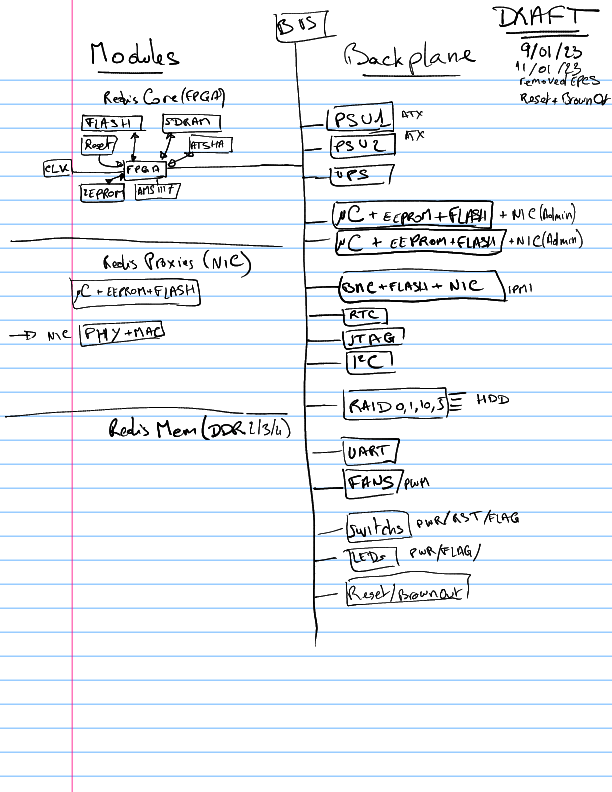

The size has respect an ATX standard to fit in standard racks. Micro-ATX
https://web.archive.org/web/20120725150314/http://www.formfactors.org/developer/specs/atx2_2.pdf
It has to embed an onboard BMC/IPMI for easy management with its own dedicated NIC.
Maybe OpenBMC (https://github.com/openbmc) running on a Raspberry Compute Module 3+ (https://www.raspberrypi.com/products/compute-module-3-plus/) in a SO-DIMM form factor, with a dedicated ENC28J60 NIC (https://www.raspberrypi.com/documentation/computers/compute-module.html).
A Reset+Brown-out+Watchdog dedicated circuit
A clean reset momentary push button with NE555 debounce.
A momentary push power button (short press soft-toggles power, long press to hard power-off)
with battery (or super-capa), updated by the microcontrolers, from the network, with NTP
It has 1 (or 2 for HA) hotpluggable microcontroler module. Each of them has his own dedicated NIC, as an 100M/1G/10G SFP+ module. It has to support backup and restore processes. With ATSHA, EEPROM, Flash, Clock, I2C BUS, I2C temp sensor
This document describes the server firmware design to be configured in the backplane microcontroler.
Check configure the specified FPGA with the specified (in configuration) gateware from the external flash
https://www.youtube.com/watch?v=THLdycw9-Vs
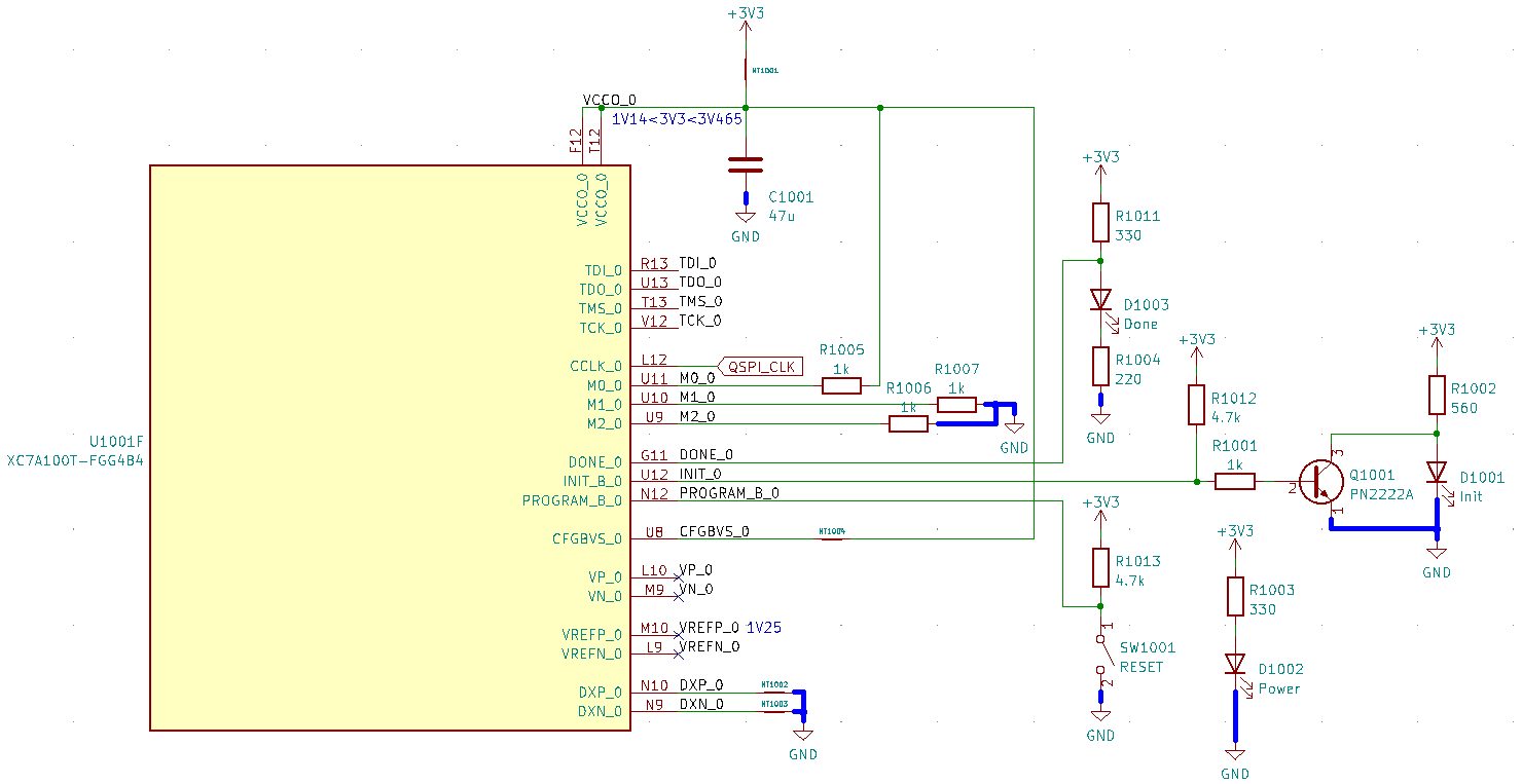
The FPGA can be configured by several means. It can received a pushed configuration from an external device such as a microcontroller, it can pull its configuration from an external device such as a flash memory, or it can be configured using the JTAG connection. Whatever happens, the JTAG always has priority. Thus, I chose to store the configuration in an external Quad-SPI flash. This FPGA device (Artix7 100T) needs 30Mbit to store the whole configuration and would need several seconds to initialize with standard SPI. I chose to use Quad-SPI flash to remain in a reasonnable configuration time, at a reasonnable cost and complexity. Unfortunately, there is a drawback, it would be too complex to access both the FPGA and the flash from the same connector (either JTAG or PCI). The Flash is behind the FPGA and not directly accessible. The programmer needs to configure the FPGA with a temporary bitstream which will act as a flash programmer, this is called indirect programming.
I need to configure the mode pins (M0, M1, M2 in bank 0) to tell the FPGA to fetch its configuration from the SPI flash. I hardwire this value because JTAG programming will still have the priority. The FPGA generate the QSPI clock signal to drive the QSPI flash on pin CCLK_0). Then I need to choose and connect the QSPI flash memory to the relevant pins in bank 14 (data lines and chip select). I do not have to care about the generated clock frequency, the FPGA will start slowly and the very first bits in the downloaded bitstream can increase the generated clock freqency dynamically. Which is very flexible to chose the actual QSPI flash chip.
The QSPI voltage levels have to be consistent across the different pins (CCLK_0 on bank 0, and the other pins on bank 14), the banks need to have the same voltage, at least during the configuration stage. I chose to power the banks 0, 14 and 15 (side effect) at 3.3V, This range is configured with the CFGBVS pin.
The PROGRAM pin acts as a reset an reacts to a pulse (it can not keep the FPGA in reset state). I connected it to a manual reset push button.
When the FPGA is started or reseted, before storing his configuration, it has to reset and clean its current configuration. The INIT_0 pin is switched to LOW during this cleanup and reverts to HIGH after to start the actual configuration. It is possible to keep it LOW and keep the FPGA in reset state.
Once the configuration is loaded, the DONE_0 pin is bring HIGH.
I connected LEDs to INIT_0 and DONE_0 as status indicators to follow and debug the reset and configuration stages.
| Name | Min. | Typ. | Max. | Load | Decoupling | Comments |
|---|---|---|---|---|---|---|
| VCCINT | 0.95V | 1.00V | 1.05V | 0.3-6A | 1x330uF, 6x4.7uF, 8x0.47uF | Same rail |
| VCCBRAM | 0.95V | 1.00V | 1.05V | 0.1A | 1x100uF, 2x0.47uF | |
| VCCAUX | 1.71V | 1.80V | 1.89V | 0.15-0.35A | 1x47uF, 3x4.7uF, 5x0.47uF | |
| VCCO | 1.14V | 3.465V | 0.2-2.5A | Bank0: 1x47uF, Other banks: 1x100uF, 2x4.7uF, 4x0.47uF | ||
| VMGTAVCC | 0.97V | 1.00V | 1.03V | 0.15-1A | Has to be filtered accordingly to 7 Series FPGAs GTP Transceiver User Guide (UG482) | |
| VMGTAVTT | 1.17V | 1.20V | 1.23V | 0.05-0.4A | ||
| VCCADC | 1.71V | 1.80V | 1.89V | 0.15-0.35A | ||
| VREFP | 1.20V | 1.25V | 1.30V | |||
| VCCBATT | 1.00V | 1.89V | Battery required only if encryption, otherwise : connect to GND or VCCAUX | |||
| VIN | -0.20V | VCCO+0.20V |
(1*6)+(1*.1)+(1.8*.35)+(3.465*2.5)+(1*1)+(1.2*.4)+(1.8*.35) = 17.5W
The FPGA could theorically consume approximately 17.5W with mixed voltages. The different voltages can not easily be generated directly from the available 12V. We need a first DC/DC conversion from 12V to 5-5.5V and a second from 5-5.5V to the different voltages. Thus, with an efficiency of 80% for each converter, we need approximately :
The card will also have network, RAM, SPI Flash, ... Despite the PCIe bus provided 12V/2.1A would be sufficient in most cases, I will add an extra power connector to use the ATX 12V/6.5A if available.
Decoupling capacitor recommendations (Types, ESL, ESR, and suggestions available in UG483)| Value | Package | Volts |
|---|---|---|
| 330uF | 2917 | 2.5V |
| 100uF | 1210 | 2.5V |
| 47uF | 1210 | 6.3V |
| 4.7uF | 0805 | 6.3V |
| 0.47uF | 0603 | 6.3V |
The card will be tested and used as a development board first. Thus, it needs to be configurable with a JTAG connector. The easiest way is to remain compatible with Xilinx's connector. Their ribbon cable has 14 pins, with an IDC connector. I added a very simple ESD protection.
I might switch later to a smaller JTAG connector with pogo pins, such as the TAG-Connects'
On standard (micro)ATX motherboards, there is a limited power available through the 3.3V and 12V rails. The ATX standard also includes extra 12V power connectors for graphic cards.
There are five possible power sources for the PCIe format :Thus, I choose to use a PCIe x16 connector to be safe. If the motherboard can be configured to deliver 5.5A, fine, if not, it can deliver 2.1A at least. In addition, I add an ATX 6pin connector to use it as a main power source, when connected, to avoid any stress on the motherboard.
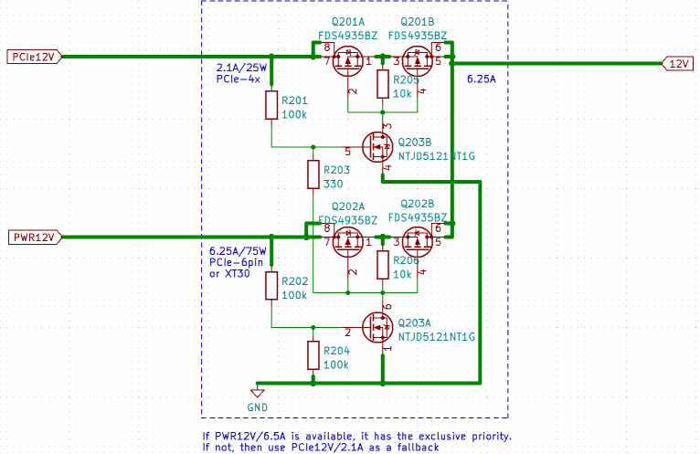
For simplicity, I do not plan to use combined power supplies. The card can use more than the 25W provided by default by the 12V PCIe connector. It needs to automatically switch to a more powerfull power source, when available. The card should use the extra connector 12V if available, then the PCIe provided 12V as a fallback, with automatic switching.
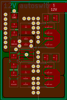
I designed an automated switching circuit, based on two P-channel MOSFETs, used as an ideal diodes to avoid voltage drop and as switches, per power source. They are drived by smaller N-Channel MOSFETs to implement the priority chain. Extra care was taken during the PCB layout design to dissipate as much heat as I can.
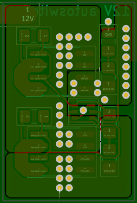
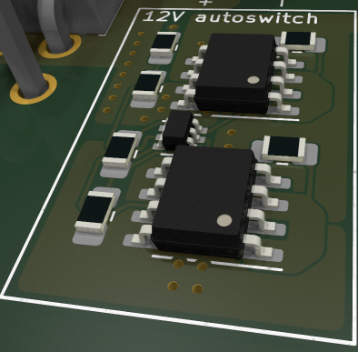
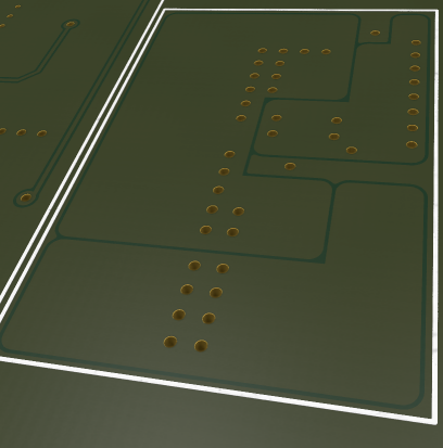
Online simulator
PCB and assembly files sent to the manufacturer: PowerSwitchModule-production.zip
The design could be simplified at the PWR12V level, given that this is the highest priority source, it should not be disabled by something else. I chose to keep it, in order to have a scalable design, in case of additional power sources, in case of a soft start, in case of a power switch, ....
Component and values choices : we have to keep in mind the limited availability of some components, currently, and the prices.
Q1A/Q1B need :I chose the same dual-PMOS chip for both Q1 and Q2, to limit the BOM length at the price of few extra cents and an oversized Q1.
Inspired by :TODO
Inductance choice : https://www.youtube.com/watch?v=ki32ZtKWe_Q
https://www.youtube.com/watch?v=FqT_Ofd54fo
The first one is fine enough and 0.20€ cheaper, still in production, available in QFN and SOIC packages, simple to implement with few components, has a programable switching frequancy between 200kHz and 4MHz. It can sustain 3.5A with a current limiter between 4 and 4.7A. Last but not least, it has an excellent documentation. Its only disadvantage is that it is an "extended part" at JLCPCB, meaning manual feeding and extra cost (x5 on average).
The third one has the huge advantage of being highly available at JLCPCB, as a "basic part" (no manual intervention, already in the feeders).
MPQ9633B:It is possible to use a complex circuit with a lot of cheap and easy to buy discrete components and simple ICs, but it means a lot of components to order, a complex routing on the PCB, a lot of very small components to solder. On the other hand, I can use few and expensive complex components, which are harder to find, but the PCB routing will be easier, there will be less soldering.
The Reducing System BOM Cost with Xilinx's Cost-Optimized Portfolio whitepaper provides SMPS suggestions (Dialog DA9062, Monolithic Power Systems MP5416, Exar/MaxLinear XRP7714, Texas Instruments TPS65023), furthermore, the Arty A7 and the AX7101 schematics also provide some good inspirations.
The main power source is the PCI express slot. I can not use the permanent 3.3V, I need to use the 12V. Either I can find a suitable component which can accept 12V input or I need to use some kind of step-down from 12V to 5.5V (I added some extra headroom for LDO dropout, in case).
- Exar/MaxLinear XRP7714 is discarded because it has only 4 outputs, and would need extra components to get all the required voltages.
- Texas Instruments TPS65023 is discarded because it can provide less current, probably not enough to make a reasonable use of the FPGA.
- Dialog DA9062 has enough outputs, enough power (up to 8.5A combined), a good set of features (watchdog, RTC, timers, power on/off sequences, ...) and a very comprehensive documentation.
- Monolithic Power Systems MP5416 has one more LDO, very interesting power (approx 15A), with a lot of features (but no RTC).
MP5416 is nearly impossible to find. Dialog DA9062 is not easy to find, but possible. That's also the PMIC used in Digilent's Arty A7 dev board.
The RAM storage has to be inexpensive and high-density, it uses DDRx standard sticks, non-EEC.
The FPGA node is too compact and the form factor is not compatible with onboard standard DDRx RAM sticks. The RAM sticks are plugged on the backplane (or on dedicated RAM extension boards) and are accessed thru DMA channels with the PCI-express bus.
The FPGA node also has a DDR3 chip for temporary and intermediate values.
ATSHA or newer
Fans are not connected or mounted on the node, but on the motherboard/backplane, to mutualize noise filtering and airflow efficiency.
Power rails ampere-meters to measure the consumed power. Temperature sensor (thermistance).
It can be used with two goals :It has a PCI express connector, at least v3.0 and at least x2 to have a bandwidth compatible with a Gigabit ethernet bandwidth.
The FPGA node has to be compatible, at least in form factor, with a standard (micro)ATX motherboard in a 1U rack. Despite it would be theorically possible to connect it to a standard motherboard, I strongly discourage this. First, you would need a kernel driver to manage and communicate with the card, but the card would have full access to the whole hardware, including the northbridge and the RAM or the southbridge and the devices, bypassing the OS kernel.
This document is the Hakeva core design for the Verilog implementation to be configured in an FPGA.
Design subject to changes:
Currently, this module implements async-reads, thus the synthesis can not infer internal BRAM blocs. The module would have to be ported to synchronous reads and the testbench updated, in order to make it compatible with internal BRAM and to make it compatible with higher frequencies.
This module is a DP-SC-SW-AR RAM. It can be preloaded with an image file to be used as a ROM (if WE0+WE1 are forced to low).
The read value is continuously assigned, thus it returns the new value, in case of writes. Its interface has to remain compatible with the external RAM (SDRAM, DDR2, DDR3, ...) design.
If both ports write to the same address concurrently, the actual stored value is undeterminated. NEVER do that !
The FIFO uses the internal RAM module design and has the same limitations in terms of size : only a power of 2. Furthermore, only ((2**ADDR_WIDTH)-1) can be used. If the FIFO is empty, it can not support a Read and a Write during the same clock cycle. The Read will return undertermined value.
FIFO inspirations :UART does not need to be complete. It only serves as a test interface to send commands to the core and receive replies, until a network layer is available/implemented.
It has to expose received data and to consume data to send in a design compatible with the TCP/IP stack implementation.
A first draft implementation is done with Nandland's sample code (https://nandland.com/uart-serial-port-module/) with two FIFOs
The cache is stored either in logic elements or in BRAM. It is preloaded at reset with an external memory (SDRAM, SRAM, DDR, ...) region. It supports both reads and writes with a write-behind logic. It needs a "drain" signal, to flush the dirty data (when the FPGA has to reset but not the RAM, without loosing data).
TODO : Rewrite this chapter to have the memory map stored at the begining of each memory chip and cached in BRAM. This will allow Full FPGA reconfiguration (partial reconfig not supported in this design) for zero-downtime/zero-dataloss bitstream upgrade.
The RAM needs to be defragmented from time to time, if not continuously. The defragmentation needs to move data blocks which are currently used by other modules. In order to avoid any kind of locking, the other module do never store the actual RAM block address, but a pointer to the address in a RAM block allocation table.
The data is stored in internal RAM blocks (M9K) but could also be stored in external RAM (DDR2/DDR3....). The RAM block allocation table is stored in internal RAM to minimize the access latency due to the communication between chips.
The RAM Block allocation table contains 512 entries x 96 bits (49152bits = less than 64KB) and is stored at the very begining of the RAM, at address 0. The maximum number of entries is a compilation parameter that can be tuned depending on the actual hardware. Each entry contain the following fixed fields :
Unused (free / available) slots reference address 0 (which is an invalid allocated block) and have the available RAM as a size. The table is initialized as follow.
| Slot# | Address | Size |
|---|---|---|
| 0 | 0000 | 1TB |
| 1 | 0000 | 0000 |
| ... | 0000 | 0000 |
| 511 | 0000 | 0000 |
Redis command decoding
Commands stored in a table with arity and branch to trigger thru a MUX.
ALU
Bus
Command pipelining
ATSHA-like crypto to crypt data at rest
ATSHA-like crypto to sign/auth the firmwares/bitstreams
Replace b-trees with n-trees and CAM-like searches, should find any key in less then logn(x)
No module support (neither preconfigured, nor dynamically configured).
Subset of Redis commands first.
One extra command returning internal statistics in a prometheus-friendly format.
see document#2
Accept incoming data and forward them, accept forwarded data and send them. The forward and accept design has to be compatible with a network connection design. This UART design is temporary, for tests and has to be replacable by a TCP/IP design.
The goal is to manage real-time background garbage collection and defragmentation. Each used memory block address is stoerd in a memory block pointer table and the IP Blocks only use indirect pointers, address in the memory block table. Thus, a physical memory block can be moved transparently, as long as the address in the block table is changed atomically.
RAM Block Address and RAM Block size
The goal is to receive a RESP encoded command from UART and reply to UART.