¶TL;DR it failed and I created another schema for the power supply. I keep this page anyway.
I will need some power for this circuit. Given that I'll have several operational amplifiers, probably some of them will need some symetrical power. It can be -5/+5, -12/+12 or anything else. I am not sure of what will be the final design, but I think that I'll be fine with -12/+12. Given that the project can embedd the power supply ... or not, I want to have a very low dependency, I don't want to depend on an external -12/+12V power supply. I want to depend to only one single voltage power supply. I chose to implement an optional 24Vdc power supply.
It has to be as clean as possible and as simple as possible. Switching power supplies need filters to avoid send noise back to the main, filter to avoid sending noise to the circuit and a shield to avoid sending noise to the whole environment. I discarded them. I chose to have a linear power supply and to make it as clean as possible.
So simple that I built it on a protoboard.
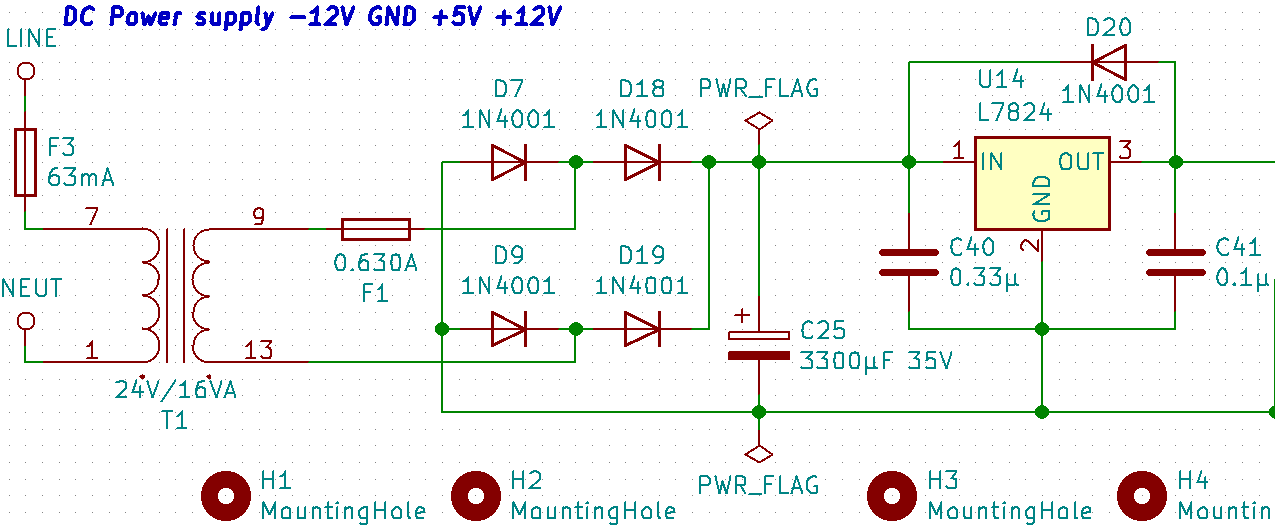
¶I already built a first prototype of the whole circuit and I know that it will consume approximately 500mA. Let's start from the need, back to the main. The smaller capacitor is not on the screenshot because it is embedded in the next circuit. It is sized accordingly to a rule : 1/10th of the transformer's filtering capacitor. We will see that this transformer capacitor is 3300µF, thus the invisible smaller capacitor is at least 330µF. I also need to have a very clean output before creating a virtual ground and powering the circuit, thus I wanted to filter 100Hz. The main in France is 50Hz, after the diodes, I'll have a 100Hz frequency and I want it to completely disapear, even if I have a regulator. I needed a 87µF capacitor, but chose to increase my expectation and to filter even more at a lower frequency, so the remaining 100Hz should be really small. I chose a 470µF for the smaller invisible filtering capacitor.
I chose a very simple and standard LM7824 to have some voltage regulation and I stupidly applied the datasheet schema by adding a 0.1µF and 0.33µF capacitor. I also added a flyback diode (D20) to avoid any capacitor from the following circuit discharging in the regulator when I switch off the power, at the end, it would destroy the regulator's transistors. Thus, when I switch off the main, the capacitors will discharge and use the D20 diode as a shortcut, protecting the regulator. Despite I don't think that this is needed, I was too lazy for the calculations and added a small TO-220 heatsink on the regulator with some thermal grease.
I chose a 3300µF for C25 because I have 32Vac at 100Hz after the rectifier diode bridge and I wanted to have very low ripples. The regulator needs to have at least 27Vdc to provide 24Vdc. Thus, I can loose up to 5V. I made my calculations based on less. C=I.*T/Vdrop, I is the current consummed by the circuit, I know that it will be approximately 0.5A and that the transformer will not be able to provide more than 0.630A. T is the time of the period in second for the source. In France, the main is at 50Hz, but after the rectifier bridge, it is 100Hz, so 0.01s. Finally, I don't want the voltage to be lower than 30V, thus the drop is 2V. C = 0.630A*0.01s/2V = 0.00325F = 3.25mF = 3500µF. With 3300µF, the voltage will be slightly lower than 30V at 100Hz, if and only if the circuit draw 0.630A, which should not be the case.
I have 34Vac at 50HZ after the transformer. I need to have DC current, thus I don't want the negative voltage. Whatever voltage (positive or negative) you apply to the bridge, you will have to go through 2 diodes. Each diode has a voltage drop of 1V, it means that from 34Vac (24Vac RMS) at 50Hz, I'll have 32Vac (22Vac RMS) at 100Hz after the bridge. That is the price to pay. I chose standard and cheap 1N4001 diodes because I can affort the voltage drop in my circuit and thay can easily handle the needed current. Let's go !
I chose this one because it was available at Farnell's and the voltage and the current are enough for my need. The datasheet asked to have a protection fuse of 0.630A after the trnsformer, thus I included it. I found that a protection fuse before would be overkill and did not include it. I'll only have a switch.
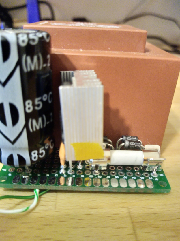
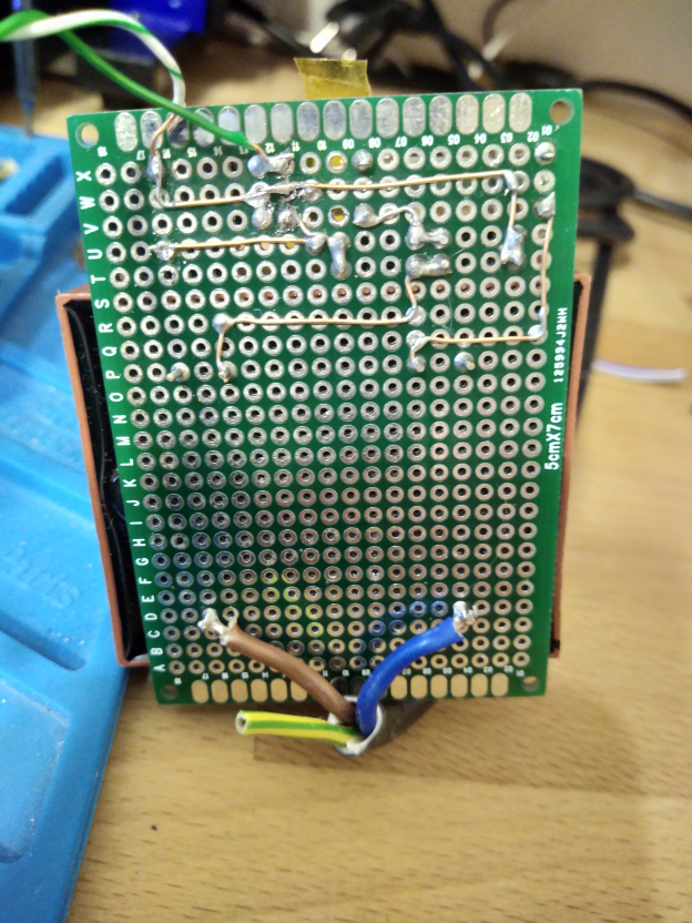
¶Nothing special here, I used the prototype board that I had instead of a clean PCB. I only have 10 components to solder on it and it fits. I designed a PCB for this part, too, but not yet built it. I can only show 3D previews.
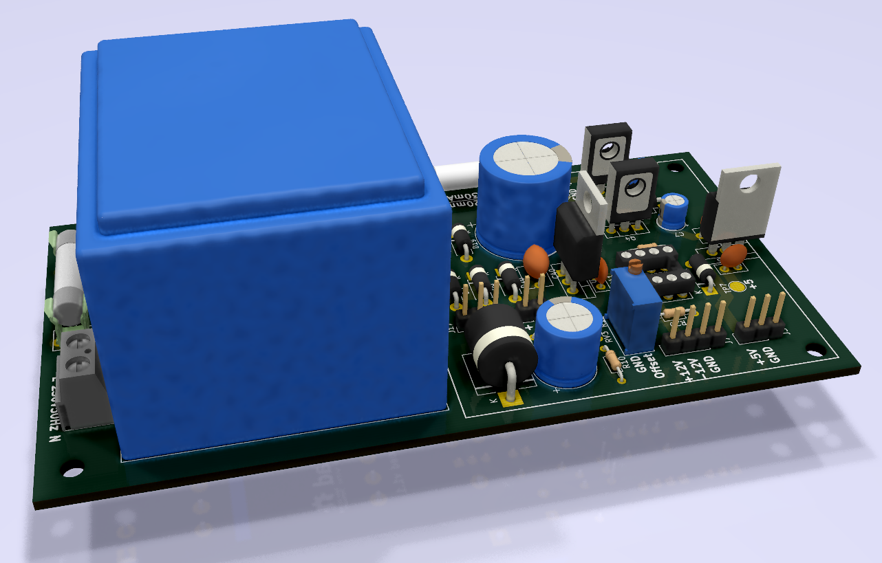
This part is critical. I need to provide a clean regulated symetrical -12V/+12V to some of the operational amplifiers and +5V th the digital part. Thus, I created a virtual ground right in the middle of the 24Vdc input and then a +5V referenced on the -12V. It was possible to generate 5V from the GND/+12V, I would have the same GND for all the rails, but I would draw more on the +12V rail than on the -12V one, it would be unbalanced and would make one of the transistors warmer than the other.

First, the previous main to 24V board is optional, any one can build his own or use an external standalone one. In my case, I'll probably power the circuit with one of my bench PSU. Thus, I included a connector J17. Pin1 is not connected, it will be blocked on the female side to avoid any mistake when pluging.
I need a shiny power LED ;) I chose to use a red one (D3) and calculated his resistor (R7) to limit the current.
I want t be protected aganinst mistakes, the pin header should protect the circuit against polarity inversions, if I use the special female plug... And nothing protects against a bad setting with higher voltage than 24V. I included a TVS, it will help to protect against reversed polarity, and high voltages. It acts as a Zener diode, with higher absolute maximums and with a prefered failure to short-cut. If I overload it, it will cut the voltage to 24V and if it is really too much, it will fry continue to short + and -. Some altruist suicide.
Finally, as I explained in the previous part, I need a filtering capacitor with approximately 1/10th of the main filtering capacitor. I prefer to embedd this one in the symetrical power schema, it will be here even if someone (including me) choose to not build the main power supply. It is sized to filter the remaining 100Hz even under full load at 630mA.
I will not detail everything here because I voided this design. Here is why. Everything is fine for the -12V/VGND/+12V. The issue arose when I wanted to generate 5V.
In this scenario, the good point is that GND is the same for -12V, +5V and +12V, the whole project will have a single GND. But With this design, the 5V regulator draws current from the +12V rail to the GND rail, consumming more on this rail than on the -12V rail, thus Q4 needs to let this extra current go back to the -12V rail to keep GND in the middle. It will be hot and dissipate a lot. I can use power resistors to artificially consume current between GND and -12V, but this is not a clean solution and I would need to dissipate 1W for nothing.
I would have the same issue, this regulator would need current from GND and Q3 would have to let current go through it, would get hot... Furthermore, this 5V would be referenced to -12V. I would have 5V between -12V and -7V. Not ideal, I would have half of the project powered by -12V/-7V (5V) and the other half powered by -12V/GND/+12V. A mess, I'd probably mix the grounds somewhere and make some magic smoke.
This one is good in terms of heat, It would draw the current from the +12V and would return it to the -12V, Q3 and A4 would be cold. But I would still have 5V referenced to -12V. Too dangerous.
Now that I understood the advantages and drawbacks, I decided to voided this whole design and to restart from a dual-coil transformer design. I learnt a lot during this experimentation and I hope that this last chapter will help you to understand the limits of such a design and choose it or discard it depending on your needs. In my case, it was inappropriate.
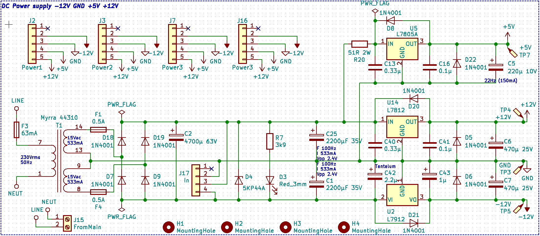
After a first failure (Discarded power supply with virtual ground), I decided to use a dual-coil transformer wit three regular voltage regulators. Thus, I redesigned the rectifier part and the regulation part.
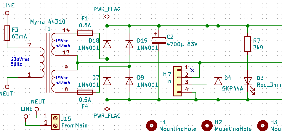
I need to generate -12V and +12V, the regulators need at least 2V more on their input than on their output, thus I'd need 14Vdc in both directions. The filtering capacitor can not be infinite, I sized it to have no more than 2.4V peak-to-peak after rectification, thus I'd need to have 16V redressed. The each diode in the bridge has a forward voltage of 1V and the current goes through 2 of them, ok, I need 18Vac peak-to-peak. This means 18/1.41=12.8Vrms. I could choose a dual 12V coils transformer but I would be at the limit and I would need to use a bigger filtering capacitor. I found a good candidate with two 15V coils, which will be perfect.
Each coil will produce 15Vrms and can sustain 0.533A. I joined the coils to have a big 30Vac 533mA coil with a central point. This central point is my ground, each end of the coil produce 15Vac with 180° of phase difference (the voltage of one is the opposite of the other). This goes through a rectifier diode bridge. I chose 1N4001, they can handle 1A and 50Vpp, 30Vac means 42Vpp. Depending on the manufacturer, the forward voltage is between 1V and 1.1V. The current will loose 2.2Vpp max when going through this bridge.
I used a first big capacitor as a first level of filtering. It had to support 30Vac (42Vpp), I chose 63V. And I used the formula C=I.T/Vdrop to calculate its capacity. C is the capacitor value in Farad, I is the maximum current drawn in Ampères, T is the period time in seconds, and Vdrop is the maximum acceptable voltage drop. I=500mA, the main frequency is 50Hz in France, this means 100Hz after rectification, thus T=0.01s, The regulators input need to be approximately 3V over their output, meaning 15V. I need a clean 30Vdc here. Despite I could accept 10V drop, I oversized to have 1V drop and I'll have a good clean current to feed the regulators. Given that this capacitor is oversized and that I will have extra capacitors behind, I chose the closest smaller standardized value : 4700µF. In theory, if the project draws 533mA, the voltage should remain between 42.30Vac and 41.41Vac, 30Vrms and 29.38Vrms, which is more than acceptable. The important thing here is to have a 63V capacitor minimum.
I decided to add a connector for two reasons :I'm human, our world is not perfect and I can make mistakes, I added a TVS (D4) to protect against reversed polarity and overvoltage peaks. Finally, I like to know when each circuit stage is healthy, thus I added a power status LED (D3) with a current limiting resistor (R7). The resistor is sized to limit the current to 10mA, this tradeoff should be enough to be visible but not consuming to much.
At the very begining of the regulation, I added filtering capacitors to polish the initial filtering. I chose two smller capacitors sized to filter the rectification bridge frequency under 533mA : 2200µF. At the end, the voltage should be very stable, at 40Vdc. These capacitors need to be 35V minimum. They will have to manage 20Vdc.
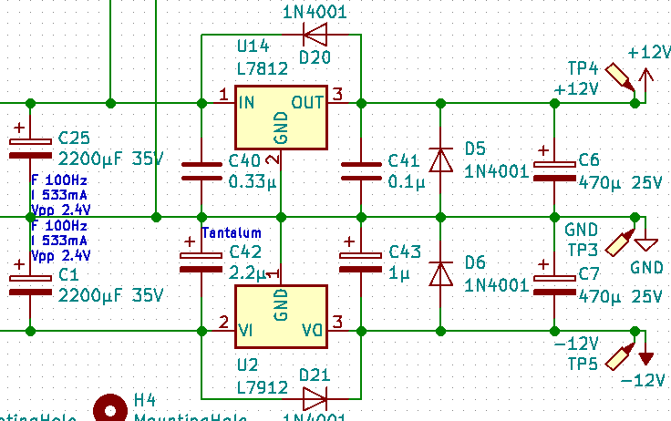
I designed the -12V/GND/+12V schema using the very standard and well known LM7812/LM7912 regulator pair and I followed the applications notes and recommendations from the datasheets (need to read carefully the 7805 7812 7824, 7905, 7912, 7924 datasheet from different manufacturers). I added a flyback diode on each regulator (D20/D21) to protect the regulators against capacitor discharge when switching off. I also added output capacitors (C6/C7) to filter any remaining noise and to help the regulators in case of current peak. These capacitors have to manage 12Vdc and I chose to use 25V capacitors for safety. I needed to add flyback diodes (D5/D6) to protect the regulators from these capacitors.
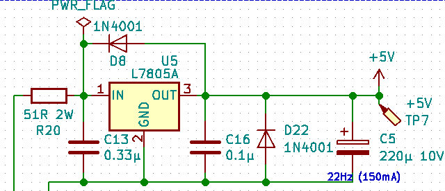
This design is nearly the same with some adjustments.
First, I did not use the regulated +12V to generate the 5V, this would make the 7812 work more than the 7912. I prefered to have a bigger drop to 5V from the 20V source. In order to save some dissipation, I used a power resistor (R20) in front of the LM7805. The LM7805 has to provide 5V from 20V, for 150mA (I approximately know the project consumption), it needs 8V to operate. The resistor has to drop 12V when drawing 150mA. I could use 80R (12/0.150) and it would dissipate 1.8W (80*0.150²) but I prefer to be careful in case of current peak, in case of 200ma, the resistor would have to dissipate 3.2W and I prefered to remain under 2W resistors. 51R semt to be a good tradeoff : in case of current peak (200mA), it would drop 10V (within the regulators limits and only .75W remaining to dissipate by the regulator) and dissipate 1.56W, under normal current (150mA), it will drop 7.6V and dissipate 1.14W.
Of course, 5V regulation also have a flyback diode (D8), a buffer capacitor (C5) and a regulator protection diode (D22) against C5.
I am 44 years old and really started electronic 3 years ago to build my own home automation modules (commercial ones are too expensive). So, I have very limited knowledge, skills, experience, money and devices. I discovered kicad 2 years ago. This will be my second real project.
All of these helped me to design my own device, as I did want to understand and not to reproduce.
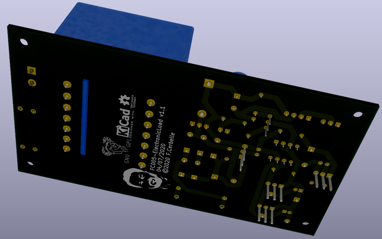
I design embedded PCB based on MySensors for my home automation system. I want some of them to run on battery and to use very low energy. Thus, I sometimes need to evaluate the power regulation part of my circuits. Some other circuits are powered from buck or boost components, or from mini switching power supply that I need to evaluate, too. I need an electronic load for that.
I am a subscriber of the French Cyrob's Youtube channel and facebook group. He often uses his commercial electronic load. Commercial products are quite expensive. I began to investigate electronic load few month ago and found Jasper's and its derivatives, or Wingman27's. There are not so many online. I also found a very old Elektor article to build one 1000W electronic load with 10 2N3055 transistors.
At the end, none of them were perfectly fitting my needs but I learnt a lot during this investigation. Thus I decided to design my perfect electronic load by myself (Schema, PCB, enclosure, firmware). This post serie describes this process and the build.
It was hard to precisely define my needs in terms of maximum ratings, thus I chose to use the same as Cyrob's Electronic load as a base : 150V, 30A, 150W. It is oversized and will give me some security headroom. My bigger bench power supply is 50V 20A, so I have very little chance to need a more powerful electronic load. Even if I manage to have only 50% of the specifications, this will satisfy my need. This is my very first complex project, after all !
Must have:Regarding the providers Banggood, JLCPCB and LCSC, this post is NOT SPONSORED at all and is independant
I initially wanted to adapt Elektor's schema, but it has intellectual property rights and I would not be able to freely share my derivated work. Cyrob also made a very simple example, way too simple regarding my wishes and I wanted to design it by myself.
I wanted to use Chinese Voltmeter/Ammeter modules, but most of them dont support so many Amps and Volts. Furthermore, this design has to be reproductible, with standard components.
Version Française sur mon blog: http://fcerbell.github.io
I needed a small electronic load, I wanted to have one. Even the smallest are way too expensive for my usage and miss a lot of wished features. Thus, I specified high ratings and numerous features, way over my needs, even if I meet 50% of the specs, this will be more than my actual need.
Discarded power supply with virtual ground
Internal symetrical power supply
Current feedback circuit
Mosfet driver circuit